PCB Design Services
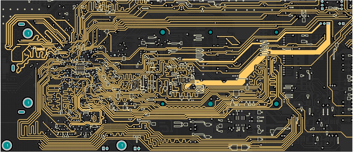
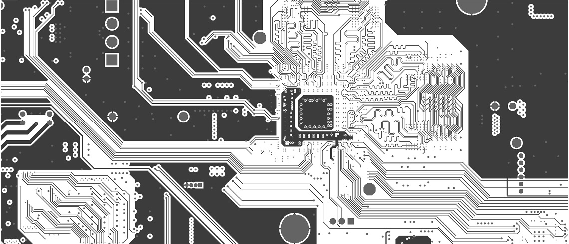
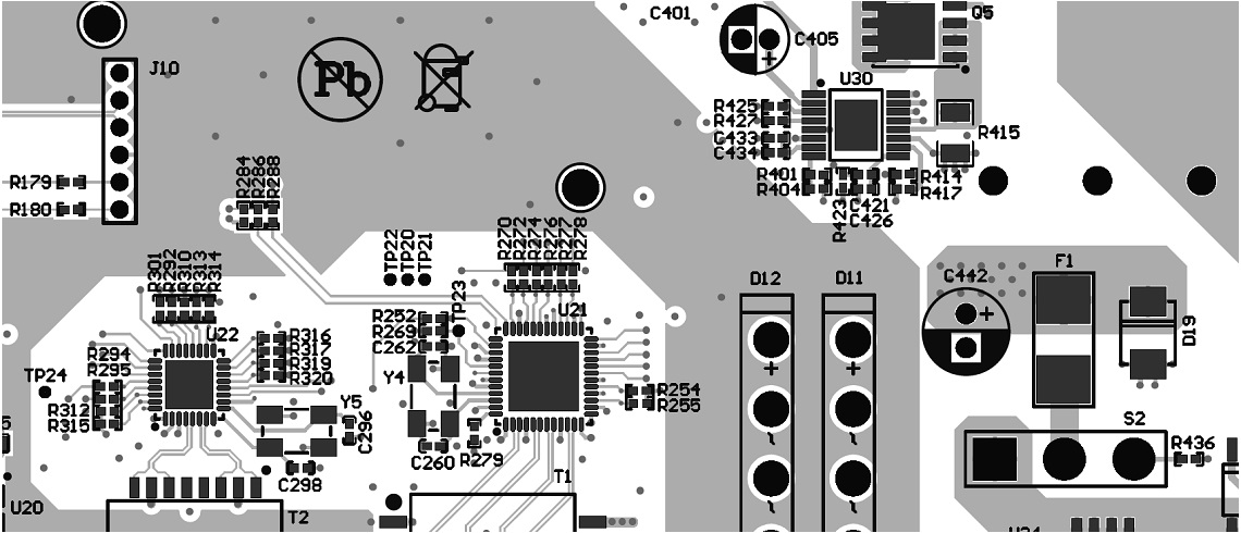
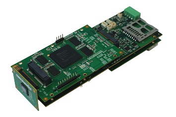
SpecForge affords high-quality PCB services, including PCB layout engineering. We have experience with various PCB CAD systems, but recently we prefer to implement projects in Altium Designer.
During the development of your product, our PCB designers work closely with electrical engineers to ensure that the location of components and their designators correspond to the requirements of the circuit and structural parts of the project. We also cooperate with manufacturers that provide the efficient assembly support and reduce marriage output during production.
If you need help in choosing a PCB vendor, we have relationships with a large number of production houses and can find the best offer to PCBs, leaving you free to focus on the core of your design project.
- High density SMT designs with any types of components cases
- High speed analog-digital PCB on one board
- Analog PCB designs, EMI provision
- High speed, multi-layer digital PCB design
- High Density Interconnect (HDI) Designs with micro vias, Via-in-Pad, laser micro vias, buried and blind via technology
- DDR, DDR2, DDR3 memory
- Impulse power supply circuits layout
- Bus routing, differential pair routing expertise, matched lengths
- Signal integrity issues to meet your digital design needs (tuned traces, diff pairs...)
- Drill, panel and cutout drawings designed
- PCB Layer management for signal integrity and impedance control
- Flex PCB, metal PCB
- Complete assembly drawings
- Creating the production documents

Information needed to do PCB Layout Design
Short description of the project
Schematic. Design Capture/View, DxDesigner or OrCAD Capture format is preferable. If it is a re-engineering project of an older existing design, do provide older schematics and other information
Bill of materials (part number, manufacture) in text or xls format
Data/Specification sheet for specific components or web URLs for them
PCB type (PCI, mini PCIe or other) or board outline with size. Desired number of layers, material type, board thickness, keep out areas, position of mounting holes and list of components which are fixed. DXF format is preferable
Special custom design rules and request that need to be followed in design. This will include all the design and routing requirements, testability, critical signals, minimum spacing, impedance matching requirements, differential pairs and others
